Wang 600 RAM Testing
Next Log Entry
MOS RAM Basic Tests
Testing so far has demonstrated that after PRIME is released the ROM address lines show a sequence of addresses that are similar to those seen in an emulated Wang 600. This suggests that the ’next instruction’ bits of the ROM and their associated logic circuits are significantly functional. Microcode appears to be running but the machine shows no function so there must be errors in other bits in the ROM, or the microcode engine, or perhaps in the RAM.
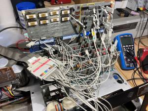
The 6183 RAM board uses early Mostek 4008P 1K x 1 bit MOS dynamic RAMs. DoPECCs Wang 600 has two of a possible 4 banks of chips populated, for a total of 2K 4-bit words.
RAM Power Saving

It seemed important to check that this basic function was operating, without correct power no RAM can function.Setting up the storage scope on the RAM power lines demonstrated that the -12 was switching in a manner that seemed reasonable.
RAM Address and Data Testing
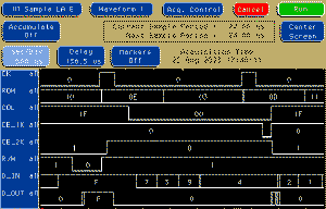


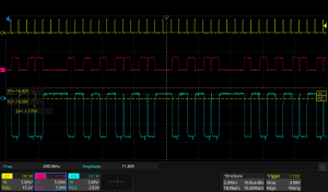
The RAM Column Address lines alternated between 0x00 and 0x1F. This was accepted as showing some kind of dynamic activity.
Scrolling through the tracings showed a scattering of RAM address and data in/out activity, suggesting that the RAM was producing data of some sort.
Later discoveries were to show that more attention should have been given to the Column Address Lines that only showed ‘all on’ or ‘all off’
Previous Log Entry Back to Log Index Next Log Entry